- 您现在的位置:买卖IC网 > Sheet目录1214 > EVAL-ADE7878EBZ (Analog Devices Inc)BOARD EVAL FOR ADE7878
�� �
�
�ADE7854/ADE7858/ADE7868/ADE7878�
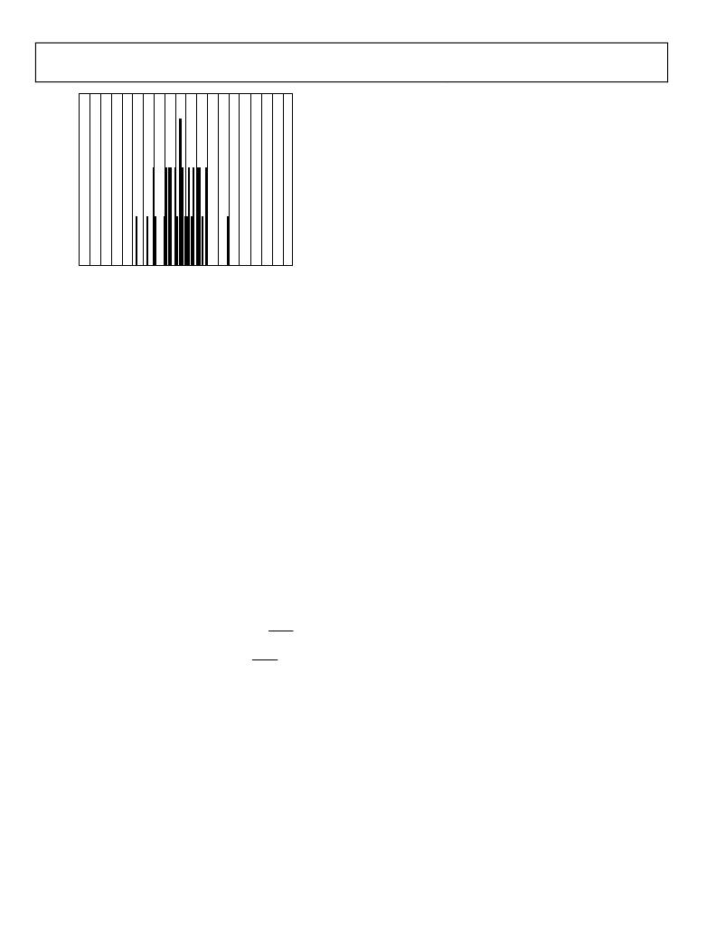
�–50� –45� –40� –35� –30� –5� –20� –15� –10� –5� 0� 5� 10� 15� 20� 25� 30� 35� 40� 45� 50�
�HOT� TEMPERATURE� COEFFICIENT� (ppm/°C)�
�Figure� 58.� Histogram� of� the� Reference� Drift� from� 25°C� to� 85°C�
�Because� the� reference� is� used� for� all� ADCs,� any� x%� drift� in� the�
�reference� results� in� a� 2x%� deviation� of� the� meter� accuracy.� The�
�reference� drift� resulting� from� temperature� changes� is� usually� very�
�small� and,� typically,� much� smaller� than� the� drift� of� other�
�components� on� a� meter.�
�The� ADE7854� /� ADE7858� /� ADE7868� /� ADE7878� use� the� internal�
�voltage� reference� when� Bit� 0� (EXTREFEN)� in� the� CONFIG2�
�register� is� cleared� to� 0� (the� default� value);� the� external� voltage�
�reference� is� used� when� the� bit� is� set� to� 1.� Set� the� CONFIG2� register�
�during� the� PSM0� mode;� its� value� is� maintained� during� the� PSM1,�
�PSM2,� and� PSM3� power� modes.�
�DIGITAL� SIGNAL� PROCESSOR�
�The� ADE7854� /� ADE7858� /� ADE7868� /� ADE7878� contain� a� fixed�
�Data� Sheet�
�memory� RAM� are� initialized� at� 0,� their� default� values,� and� they�
�can� be� read/written� without� any� restriction.� The� run� register,�
�used� to� start� and� stop� the� DSP,� is� cleared� to� 0x0000.� The� run�
�register� needs� to� be� written� with� 0x0001� for� the� DSP� to� start�
�code� execution.�
�To� protect� the� integrity� of� the� data� stored� in� the� data� memory�
�RAM� of� the� DSP� (addresses� between� 0x4380� and� 0x43BE),�
�a� write� protection� mechanism� is� available.� By� default,� the�
�protection� is� disabled� and� registers� placed� between� 0x4380� and�
�0x43BE� can� be� written� without� restriction.� When� the� protection�
�is� enabled,� no� writes� to� these� registers� is� allowed.� Registers� can�
�be� always� read,� without� restriction,� independent� of� the� write�
�protection� state.�
�To� enable� the� protection,� write� 0xAD� to� an� internal� 8-bit�
�register� located� at� Address� 0xE7FE,� followed� by� a� write� of� 0x80�
�to� an� internal� 8-bit� register� located� at� Address� 0xE7E3.�
�It� is� recommended� to� enable� the� write� protection� after� the�
�registers� have� been� initialized.� If� any� data� memory� RAM� based�
�register� needs� to� be� changed,� simply� disable� the� protection,�
�change� the� value� and� then� re-enable� the� protection.� There� is�
�no� need� to� stop� the� DSP� to� change� these� registers.�
�To� disable� the� protection,� write� 0xAD� to� an� internal� 8-bit�
�register� located� at� Address� 0xE7FE,� followed� by� a� write� of� 0x00�
�to� an� internal� 8-bit� register� located� at� Address� 0xE7E3.�
���follows:�
�function� digital� signal� processor� (DSP)� that� computes� all� powers�
�and� rms� values.� It� contains� program� memory� ROM� and� data�
�memory� RAM.�
�The� program� used� for� the� power� and� rms� computations� is�
�stored� in� the� program� memory� ROM� and� the� processor� executes�
�it� every� 8� kHz.� The� end� of� the� computations� is� signaled� by�
�setting� Bit� 17� (DREADY)� to� 1� in� the� STATUS0� register.� An�
�interrupt� attached� to� this� flag� can� be� enabled� by� setting� Bit� 17�
�(DREADY)� in� the� MASK0� register.� If� enabled,� the� IRQ0� pin� is�
�set� low� and� Status� Bit� DREADY� is� set� to� 1� at� the� end� of� the�
�computations.� The� status� bit� is� cleared� and� the� IRQ0� pin� is� set�
�to� high� by� writing� to� the� STATUS0� register� with� Bit� 17� (DREADY)�
�set� to� 1.�
�The� registers� used� by� the� DSP� are� located� in� the� data� memory�
�RAM,� at� addresses� between� 0x4380� and� 0x43BE.� The� width� of�
�this� memory� is� 28� bits.� Within� the� DSP� core,� the� DSP� contains� a�
�two� stage� pipeline.� This� means� that� when� a� single� register� needs�
�to� be� initialized,� two� more� writes� are� required� to� ensure� the�
�value� has� been� written� into� RAM,� and� if� two� or� more� registers�
�need� to� be� initialized,� the� last� register� must� be� written� two� more�
�times� to� ensure� the� value� has� been� written� into� RAM.�
�As� explained� in� the� Power-Up� Procedure� section,� at� power-up�
�or� after� a� hardware� or� software� reset,� the� DSP� is� in� idle� mode.�
�No� instruction� is� executed.� All� the� registers� located� in� the� data�
�?�
�?�
�?�
�?�
�?�
�?�
�?�
�?�
�Initialize� the� AIGAIN,� BIGAIN,� CIGAIN,� and� NIGAIN�
�registers.�
�Start� the� DSP� by� setting� run� =� 1.�
�Initialize� all� the� other� data� memory� RAM� registers.� Write�
�the� last� register� in� the� queue� three� times� to� ensure� its�
�value� was� written� into� the� RAM.� Initialize� all� of� the� other�
��exception� of� the� CFMODE� register.�
�Read� the� energy� registers� xWATTHR,� xFWATTHR,�
�xVARHR,� xFVARHR,� and� xVAHR� to� erase� their� content�
�and� start� energy� accumulation� from� a� known� state.�
�Clear� Bit� 9� (CF1DIS),� Bit� 10� (CF2DIS),� and� Bit� 11�
�(CF3DIS)� in� the� CFMODE� register� to� enable� pulses� at�
�the� CF1,� CF2,� and� CF3� pins.� Do� this� initialization� last,�
���Enable� the� write� protection� by� writing� 0xAD� to� an� internal�
�8-bit� register� located� at� Address� 0xE7FE,� followed� by� a� write� of�
�0x80� to� an� internal� 8-bit� register� located� at� Address� 0xE7E3.�
�Read� back� all� data� memory� RAM� registers� to� ensure� they�
�were� initialized� with� the� desired� values.�
�In� the� remote� case� that� one� or� more� registers� are� not� initia-�
�lized� correctly,� disable� the� protection� by� writing� 0xAD� to�
�Rev.� H� |� Page� 42� of� 100�
�发布紧急采购,3分钟左右您将得到回复。
相关PDF资料
EVAL-ADE7880EBZ
BOARD EVAL FOR ADE7880
EVAL-ADE7953EBZ
BOARD EVAL FOR ADE7953
EVAL-ADF4002EBZ1
BOARD EVAL FOR ADF4002
EVAL-ADG788EBZ
BOARD EVALUATION FOR ADG788
EVAL-ADM1021AEB
BOARD EVAL FOR ADM1021
EVAL-ADM1023EB
BOARD EVAL FOR ADM1023
EVAL-ADM1031EB
BOARD EVAL FOR ADM1031
EVAL-ADM1062TQEBZ
BOARD EVALUATION FOR ADM1062TQ
相关代理商/技术参数
EVAL-ADE7880EBZ
功能描述:BOARD EVAL FOR ADE7880 RoHS:是 类别:编程器,开发系统 >> 评估演示板和套件 系列:* 产品培训模块:Obsolescence Mitigation Program 标准包装:1 系列:- 主要目的:电源管理,电池充电器 嵌入式:否 已用 IC / 零件:MAX8903A 主要属性:1 芯锂离子电池 次要属性:状态 LED 已供物品:板
EVAL-ADE7880EBZ
制造商:Analog Devices 功能描述:ADE7880, ENERGY METER, 3 PH, SPI, I2C, E
EVAL-ADE7913EBZ
制造商:AD 制造商全称:Analog Devices 功能描述:3-Channel, Isolated, Sigma-Delta ADC with SPI
EVAL-ADE7953EBZ
功能描述:BOARD EVAL FOR ADE7953 RoHS:是 类别:编程器,开发系统 >> 评估演示板和套件 系列:- 标准包装:1 系列:PSoC® 主要目的:电源管理,热管理 嵌入式:- 已用 IC / 零件:- 主要属性:- 次要属性:- 已供物品:板,CD,电源
EVAL-ADF4001EBZ2
制造商:Analog Devices 功能描述:Evaluation Board For Pll Frequency Synthesizer 制造商:Analog Devices 功能描述:ADF4001 PLL SYNTHESIZER EVAL BOARD
EVAL-ADF4002EB1
制造商:Analog Devices 功能描述:EVAL BOARD - Bulk
EVAL-ADF4002EBZ1
功能描述:BOARD EVAL FOR ADF4002 RoHS:是 类别:编程器,开发系统 >> 评估演示板和套件 系列:- 产品培训模块:Obsolescence Mitigation Program 标准包装:1 系列:- 主要目的:电源管理,电池充电器 嵌入式:否 已用 IC / 零件:MAX8903A 主要属性:1 芯锂离子电池 次要属性:状态 LED 已供物品:板
EVAL-ADF4007EBZ1
功能描述:BOARD EVALUATION FOR ADF4007EB1 RoHS:是 类别:编程器,开发系统 >> 评估演示板和套件 系列:- 标准包装:1 系列:PSoC® 主要目的:电源管理,热管理 嵌入式:- 已用 IC / 零件:- 主要属性:- 次要属性:- 已供物品:板,CD,电源